


In previous posts, we shared details about our hardware design, including our processor selection, how it will be powered (USB-C with rechargeable battery), how a customer will unlock and interact with it (fingerprint sensor or PIN), and how it will communicate with the mobile device’s app (NFC). We have even shared some pictures of early industrial design models that have helped us refine the look and feel of the device. Now that we have all our major architectural decisions finalized, we are excited to share more about the hardware design and development process in this post.
Hardware Development Process
Once we have locked the hardware architecture, our team works to identify all the possible risk areas for function, performance, usability, and reliability. We then take those risks and develop a plan to prototype, test, and iterate our design so that it will meet all of the performance and reliability targets by the time we are ready to start shipping it to customers. Our hardware development process is broken into several phases, each with a specific set of goals that helps us validate and refine the design until we produce a device that is reliable and manufacturable at scale. These phases are:
- Development ('Dev' ← where we’ve been): As soon as we have locked all our key electrical component decisions we build what we call “Dev Boards”. These are large logic boards with all of the key components that our system will have as well as many additional components that allow the electrical, firmware, and software engineers to start testing and validating that the system design works as intended and enables them to develop the device firmware and mobile software needed to implement many of the features of the product.
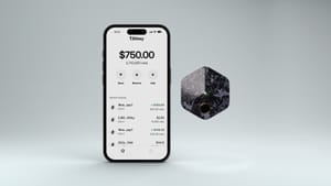
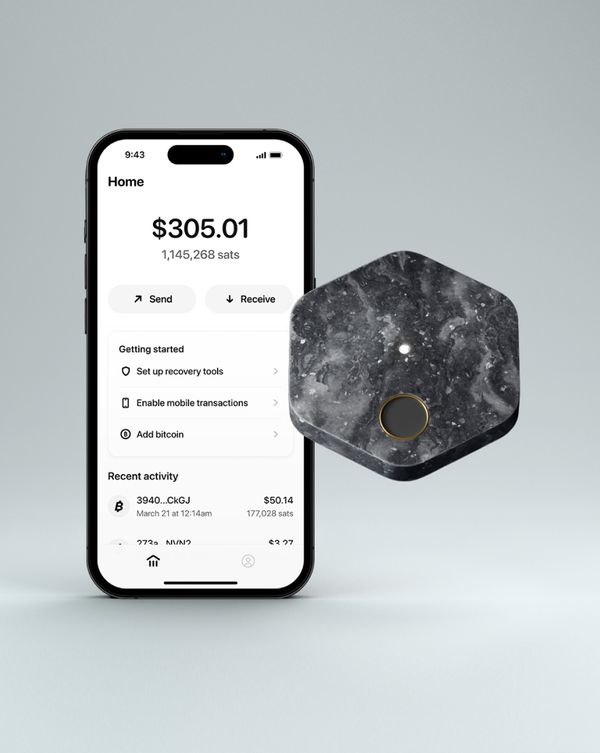
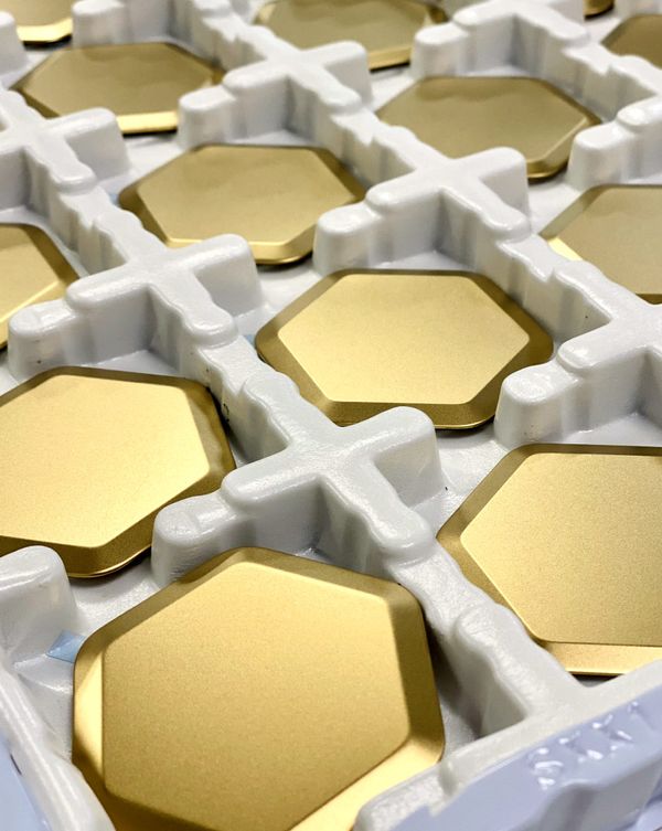
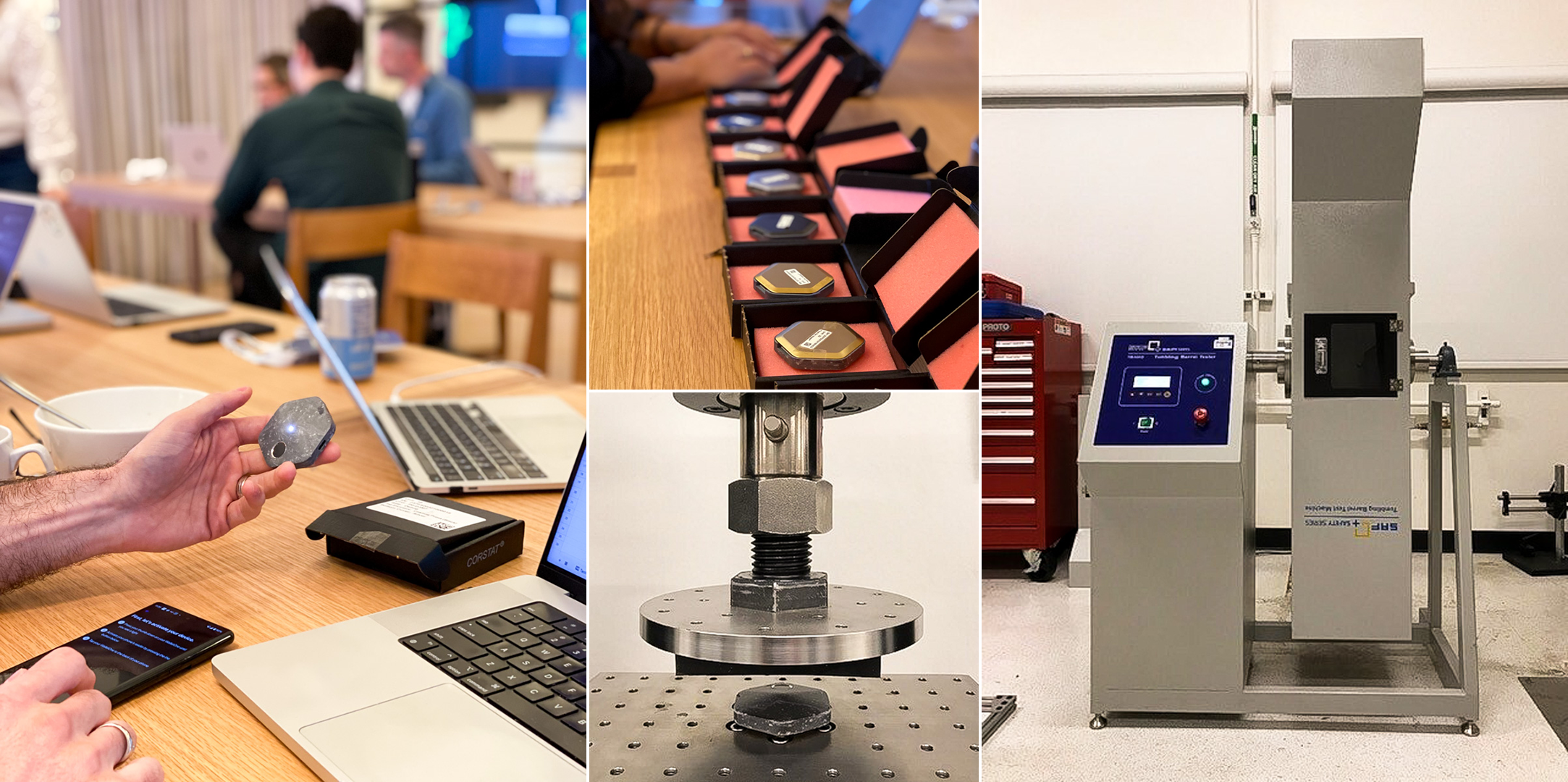
- Prototype ('Proto' ← where we are): Proto builds are the first time we build hardware in the intended form-factor. Sometimes these builds are not fully representative of our intended design or assembly, but they give us hardware that we can test and use to assess the risks we identified at the start of the project. There could be big changes to the design or assembly that come out of these learnings as we work through a majority of the reliability and test challenges in this phase. This is the phase of the project that we are currently in and is represented in the pictures below.
- Engineering Validation Test ('EVT' ← where we’re going next): EVT validates the final design using parts and assemblies made in our planned mass production process. There are sometimes small changes to the design to resolve final reliability issues and improvements to the assembly process as we prepare for mass production. This hardware is usually mature enough to enable regulatory certification testing and early customer beta testing.
- Design Validation Test ('DVT'): DVT validates our mass production manufacturing and assembly processes. We target specific yield and throughput goals and work to resolve any issues that prevent us from meeting those goals – this is our first chance to discover potential design or manufacturing issues that can only be identified at scale.
- Production Validation Test ('PVT'): PVT is the start of our mass production. We closely monitor the first set of units that come off the production line to ensure process and quality meets expectations. If needed we use this phase to qualify additional production lines and ensure yields and quality are all meeting our criteria.
First Prototypes
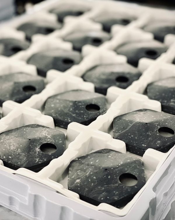
Our first hardware prototypes were a combination of units assembled by our engineering team to assess fit and function and then a larger quantity assembled by our contract manufacturer (more on this in a future post) to distribute to our team for continued firmware and software development as well as reliability testing.
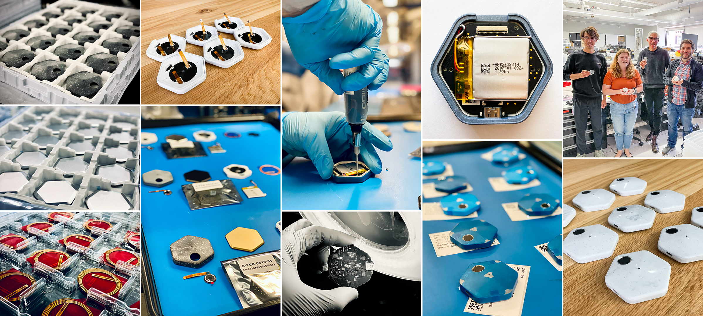
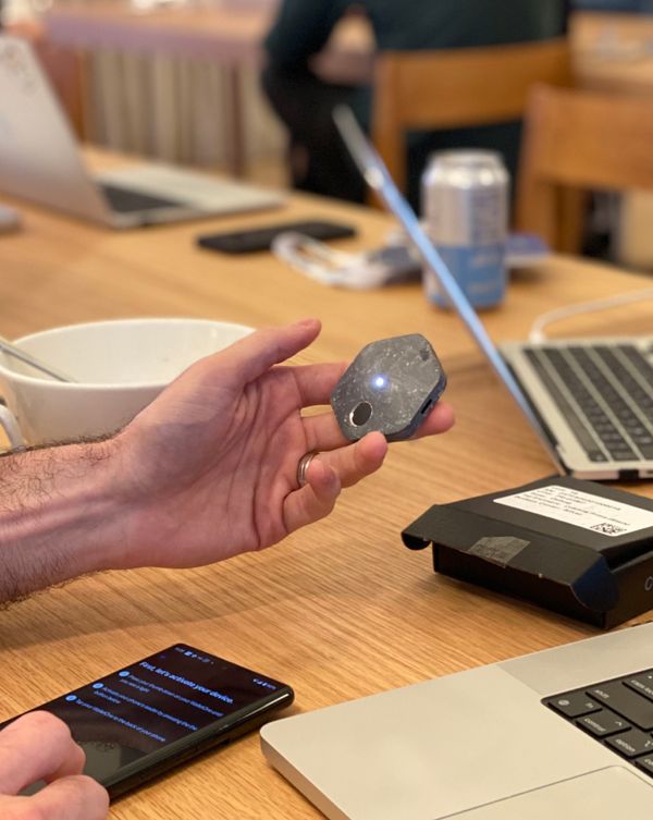
Once our first hardware prototypes were built, our team gathered to perform what we called “alpha testing.” We ran through various user flows in the mobile app to study hardware and software interaction, NFC performance with various iOS and Android devices, and user interactions with the fingerprint sensor and LED. We also sent a large quantity of units through a rigorous suite of reliability tests to tease out design weaknesses when exposed to real world environments and use cases. Our team will take the learnings of these activities, modify the electrical and mechanical designs as needed, and repeat this process of building and testing over the next few months until we pass all of our performance and reliability specifications. In a future post we’ll dive more into the reliability testing process.
How We Approach System Design
In addition to sharing our development process and as part of our goal to develop this product as transparently as possible, we’ll dive into some details about the mechanical and electrical designs of the hardware device.
Mechanical Design
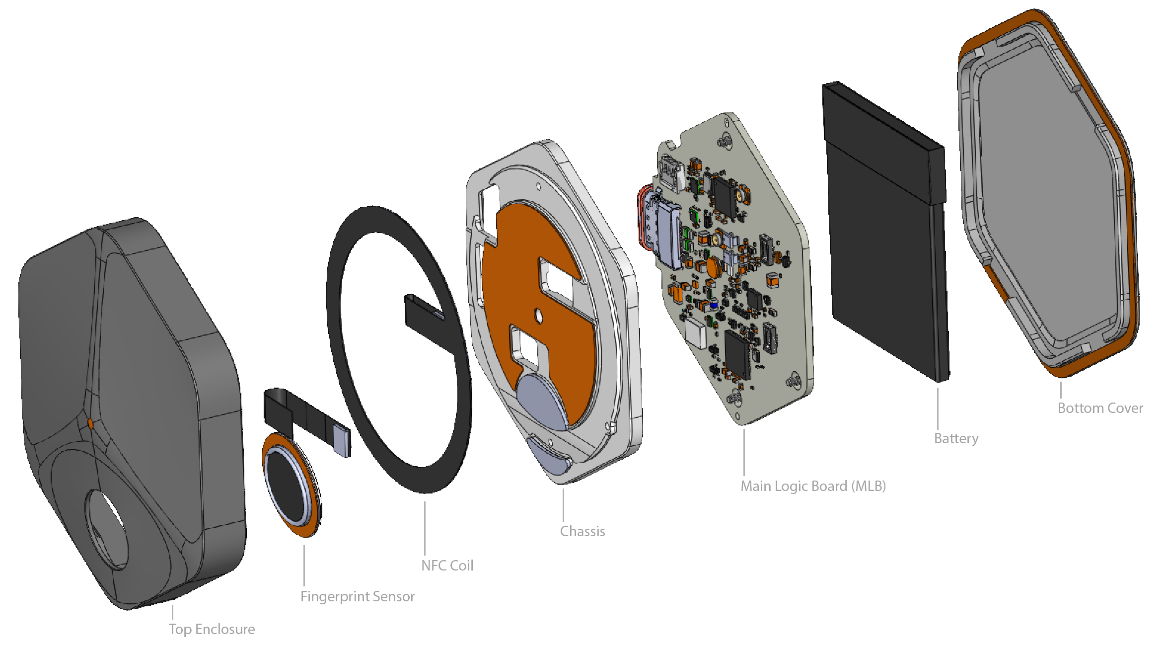
We want to build a reliable product that meets the needs of our customers and exhibits world class performance in terms of both design and manufacturing. Some of the key areas we are putting a lot of energy into getting right are focused around reliability, most notably drop testing and water ingress performance. This means looking at every part closely and optimizing for strength while maintaining our Industrial Design goals of a distinctive and trustworthy product. In some cases, this means designing custom parts where using an off-the-shelf option would be a compromise in some way. Our USB-C connector for example is a custom part we are designing with a partner to meet both our reliability and unique form factor goals. The diagram below shows a breakdown of the key components in our system:
Balancing Physical Design and Performance
The performance of a product like our wallet is not based on any single design decision, but quite literally, thousands. We look closely at the difference between the look and feel of a 0.1 vs 0.2 millimeter corner radius on the outer surface because sometimes even the tiniest details affect how our customers experience the product. Our obsession with design and performance sometimes leads us down design paths with a high degree of difficulty, but this often is the difference between an average product and a great one. The way we do this is by conceptualizing, designing, building, testing and then iterating this entire process over many cycles. We want to stress test the product in every way possible through the development process, find where weaknesses exist, and then fix them. This rigorous approach allows us to deliver an impactful product we’ve imagined for our future customers that we can be proud of. We look forward to more product testing and learnings at our upcoming build!
Electrical Design
In addition to designing and building mechanical parts, we’re also building the electrical system that lives between the mechanical design and firmware and represents the transition between the physical and virtual world. Many of the goals on the electrical side are common with those on the mechanical side – product reliability and performance are paramount. First and foremost, the electrical design must implement the physical layer of many of the envisioned features of the product, such as NFC communication, fingerprint sensing, power management, and LED behavior. Furthermore, it must function in a stable and predictable way across a variety of external and internal conditions (over a range of temperatures, humidity, voltages, etc.). The electrical components must fit in the space allotted by the mechanical design, and they must be tolerant to various mechanical stresses – like those that come with a drop on the floor or a bumpy ride in a backpack. The electrical components also define the platform that the device firmware uses to control the behavior of the product and must include features that allow the firmware to control and interpret the state of various subsystems. Additionally, the electrical system must be manufacturable, not only from a physical standpoint, but also while taking operational and logistical challenges into account. Finally, we need to ensure the selected components can actually be procured with short enough lead times to meet production volumes and at the appropriate price point for the product.
How We Meet Electrical Design Criteria
We're balancing many disparate goals when building the electrical system, and we need to validate that the choices we make achieve our design criteria and work well together in practice. To do this, we typically create:
- Clear design documentation that captures how product requirements map to engineering requirements and system architecture (example: system block diagrams)
- Engineering models that ensure the design of system is capable of meeting the intended product performance (example: a power model for the system)
- Checklists used to review the schematics and printed circuit board (PCB) design for adherence to engineering best practices, cross-functional compatibility, and manufacturability
- 3D models of the printed circuit boards that can be checked against mechanical CAD for interference issues
- An electrical validation plan that defines performance tests for each of the subsystems across a variety of conditions (example: power consumption across operating temperature range and battery voltage range)
- A reliability test plan that tests performance against environmental stresses that will occur in the field (example: electrostatic discharge – ESD)
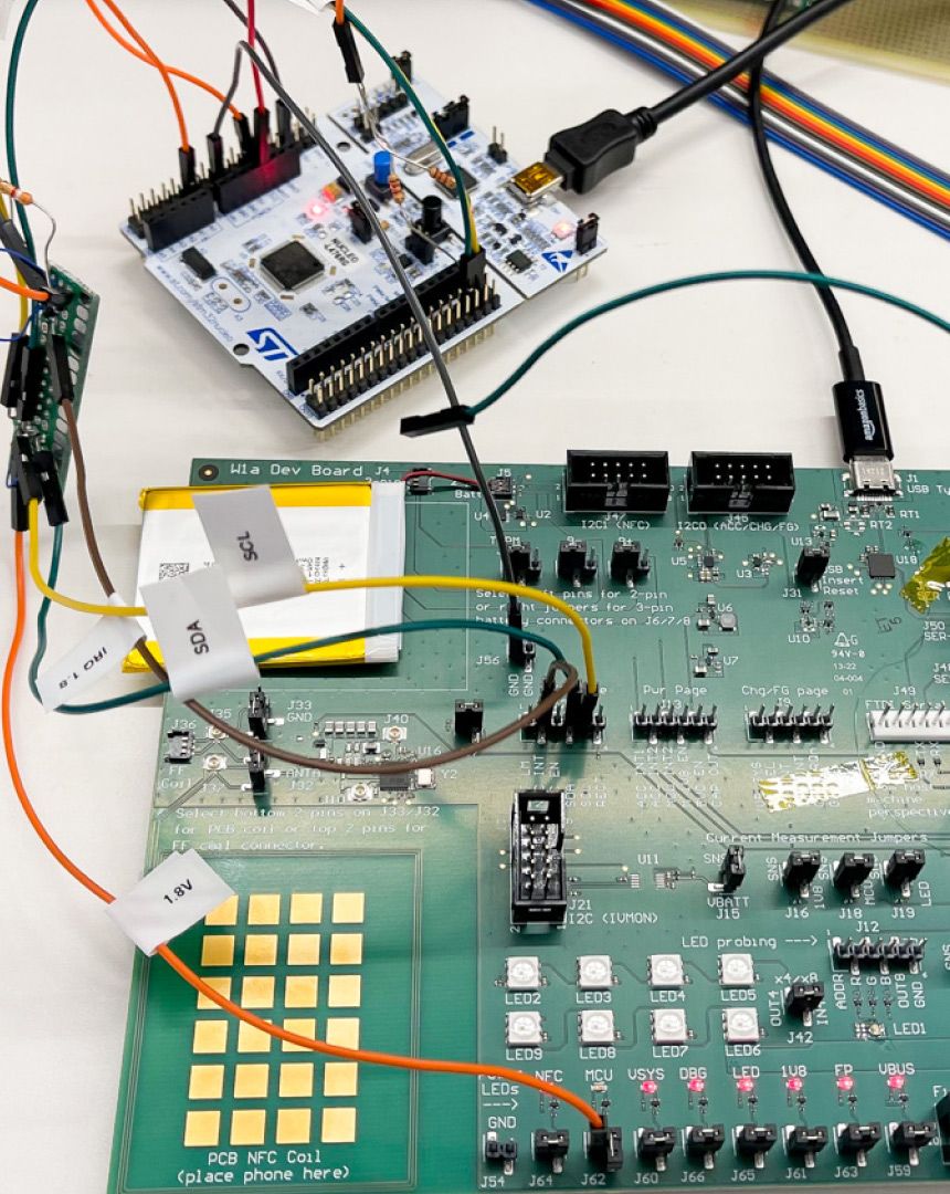
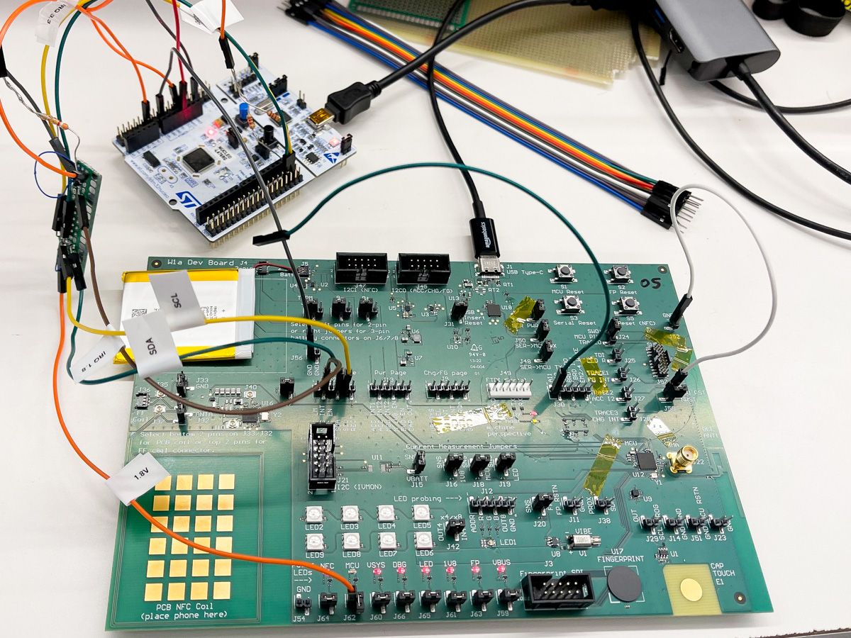
- Development tools that allow firmware developers to easily program and debug prototypes (example: breakout board with programming and serial interfaces that be connected to a host machine)
- A list of alternate sources for electrical components that can meet the design requirements in case there is difficulty procuring the primary source
Prototype Electrical Hardware
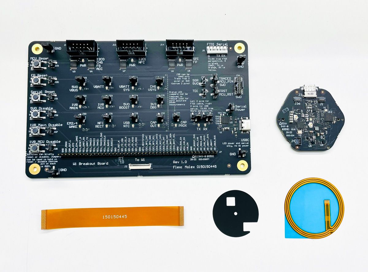
In the image below, you can see real electrical system hardware from our prototype phase. The left half of the picture shows our 'breakout' board and the 'flex' cable used to connect it to the actual wallet hardware; we use these to develop the firmware and test our design. In the lower right corner, you can see an NFC coil 'flex' and the black ferrite used to optimize the performance of the NFC channel between the hardware and phone. Finally, in the upper right is the main logic board (or "MLB"), which is the actual electrical system that goes into the finished product.
What’s Next
Our team is very excited to be able to share our journey as we strive to make the most robust, secure, open source hardware possible (look out for electrical schematics and detailed design information soon!). If you have feedback on our development process or to let us know what you want to hear about next please reach out to us at bitkey@block.xyz or on Twitter.
If this project sounds exciting to you, we are hiring! Key open roles include: